Application Notes
Voltage vs. Insulation Resistance
as applied to Backplane / Backpanel Testing
Voltage Test = Physical Spacing Test
(Dielectric Withstanding Voltage - DWV)
Voltage should be used to test that a minimum spacing between two conductors exists. We recommend that the bare board be tested as high a voltage as economically possible. Current bare board test equipment typically provides test voltages between 100 - 250 volts. With a 250 volt test, you would ensure that exposed conductors have a spacing greater than .005”.
(Typically, expect to see 50 volts per .001”, (.0254 mm), for conductors exposed to air. Soldermask and especially flowed FR-4, prepeg, provide better insulators than air, and therefore provide a much greater voltage per mil. (However, for this discussion, we will focus on external, free air conductors.)
The difference in fault coverage between 100 volts, 25 volts and 10 volts is very minimal. (Assuming that dielectric voltage is the issue, not equipment sensitivity). A 100 volt test is at best a .002” spacing test. Our experience is that any sliver or curl that is within .002” of touching another conductive spot represents a very intermittent fault. Thermal expansion of the board, shipment vibration, or just the act of plugging in the daughter card will affect the area. Furthermore, a .003” short would pass test, but could fail after shipment, once the daughter card is inserted, or when the equipment rack warms up.
For this reason, our comment is that a 100 volt test is not a true test of physical spacing. Ideally, if slivers and curls are a problem we would recommend voltage testing of 300 volts - 500 volts thereby guaranteeing free air spacing between conductors greater than .006” - .008”. (Mil standard 202 defines DWV testing at 500V, 1000V or 1500V).
To further complicate the voltage testing issue, now that passive and active components are being installed on backplanes, high voltage testing can do significantly more harm than any advantage it may have once offered. When a component is exposed to high voltage, the best case is that it fails immediately. In reality, latent defects are often induced and fail only after some time in functional burn in or once the assembly is placed in the field.
A common misconception about high voltage testing is that it is current limited, thereby limiting the collateral damage to the backplane assembly if an arc occurs. This is not true. The test equipment typically does not provide the current to sustain the arc. The capacitance present on the board sustains the arc. Even if the test equipment charged up the board very slowly, once an arc starts, all of the stored voltage is immediately discharged. The current flowing can be between tens of Amps to hundreds of Amps. There will be carbon tracks and other debris present after an arc. Sometimes the arc will alter the physical characteristics of the conductor and it will now pass a retest, even though debris is now present. This can lead to long-term failure as it provides a medium for Dendritic Crystal growth.
If the backplane failed due to spacing, this means that an arc was created. Generating an Arc on a backplane is just as bad and has the same effect as the act of “Blowing a short”. This is when a high current source is used to melt the conductive material between two traces. (Fortunately, no quality board shop “blows shorts” anymore.) Both the arc and the “blown short” leave a significant amount of debris between the two conductors which then leads to Insulation Resistance failures.
Verification of spacing failures can be very frustrating. If it is truly a close spacing failure detected through voltage tests, the verifier must have an instrument with the same voltage capabilities. If they use a standard ohm meter to verify the fault, they will not get any reading. They will be tempted to say it was a false failure as it is not verifiable and will pass the assembly. As a corollary point, if they were able to verify the failure with a standard ohmmeter, then the fault was not a spacing failure to begin with.
Insulation Resistance Test = Contamination / Cleanliness Test
Three satellites, Galaxy 4, Galaxy 7, and DBS-1 all failed in space due to electrochemical migration of tin, thereby creating a short circuit between conductors. This is not a failure only possible with satellites. Electrochemical migration is a problem that can occur with almost any electronic assembly. Electrochemical corrosion of metallic conductors and the migration of metal ions between traces and plated through holes can lead to catastrophic circuit failure.
There are two typical types of failures associated with contamination: Dendritic Crystallization Growth and Conductive Anodic Filament (CAF) Formation.
Conductive anodic filament formation is easily differentiated from dendrite growth. Dendritic growth starts at the cathode, growing tree-like dendrites across the surface of the PWB. Conductive anodic filament growth starts at the anode. Dendrite growth is a surface issue, while conductive anodic filament growth is a subsurface issue.
Dendrite and filament growth is not a new problem. Research has been going on since the early 1970’s. The problem has not gone away and is in reality more of an issue with today’s advanced technology backplanes. This is due to tighter spacing, higher density connectors, SMT fluxes, hot air solder leveling (HASL) fluids, and as always, moisture.
An Insulation Resistance (IR) test is typically one of the best ways to detect latent / residual board contaminates which promote dendrite and filament growth. (Most standards require an IR test to ensure that the trace to trace resistance is at least 10 Mohms). Fortunately, most advanced test equipment can easily test at these resistance levels without having to resort to high voltage which can damage the board and components.
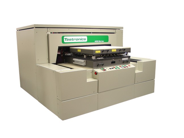
Many of the failures associated with voltage testing are actually Insulation Resistance (IR) failures, whereas the higher voltage of the test equipment provided the sensitivity to detect IR failures. A 10 volt test at 1 mAmp provides an Insulation Resistance threshold of 10 Mohms. A 100 volt test at 10 mAmps also provides a 10 Mohm threshold. The higher voltage makes the current measurement easier as there is less noise present. Unfortunately with today’s advanced backplane assemblies with their tight spacing and components, the high voltage tends to cause more damage than good. For this reason, backplane test systems were specially developed to provide sensitive current measurements without having to use high voltage. (The current Testronics backplane test systems can actually measure currents less than 100 nAmps, (resistances greater than 100Mohms) while sourcing as little as 10 volts.)
Our experience is that Insulation Resistance is a crucial test that should be performed on all backplane assemblies at the lowest possible voltage. (If active components are present, the test must be performed at .25 volts so as not to turn on and possibly damage any diode / semiconductor junctions.)
| Summary Points: |
- Bare boards should be tested at as high a voltage as economically feasible.
- If voltage is truly being used as a method of detecting physical separation between conductors, the difference between 100 volts and 10 volts is .002” of separation.
- Many older technology Test systems use voltage to increase its’ Insulation Resistance sensitivity.
- High voltage and components do not mix.
- Most voltage failures are actually IR failures. The older test equipment is made more sensitive by the increased voltage.
- Insulation Resistance is a very crucial test as it verifies the assembly is clear of contaminates.
- Contaminate detection, (IR Testing), is becoming a major factor in long term assembly reliability as contaminates are directly associated with Dendritic Crystal growth and Conductive Anodic Filament formation.
- Tier 1 backplane producers have opted to utilize Analog In-Circuit test equipment to characterize the quality of today’s advanced backplane assembly.
- Active components are tested using vectorless techniques. (Measure DVf at multiple current levels, or utilize Agilent TestJet technology.)
- Series Parallel circuits are testable due to the 6 wire guarded measurement techniques. (Almost all backplanes have pull up / pull down resistor networks which are not testable with anything less than a true In Circuit measurement system)
- Trace resistance is measurable to .01 ohms on any net with 4 or more test points. (4 wire Kelvin measurement capability)
- Insulation Resistance is testable to 100 Mohms. ( 100nAmps @ 10 Volts = 100 Mohms)
- If active components are present, the test voltage should be .25 volts to preclude any junction damage.
|
|